PCB for sale
Note these are
Rev 1 boards
€7.49
4 Available

PCB for sale
Note these are
Rev 1 boards
€7.49
4 Available
Assembled board for sale
Rev 1 Board
€21.99
1 Available

Kit for sale
Rev 1
€16.49
0 Available
Sepic UPS for the Raspberry pi

Simple UPS for the raspberry pi uses a Sepic topology
Download build manual here
The circuit described below will backup a raspberry pi for around 2 hours when fully charged with a 1500mA 4 Cell AA NiMh pack. Other cell configurations could be looked at also to provide longer if needed.
When there is a power failure (Not uncommon in the west coast of Ireland in the winter) it can be necessary to backup computers to enable them to be shutdown in an orderly manner so as not to corrupt data.
Or just survive a short outage, as I am away frequently and use the pi at home for data logging it would be convenient if I didn’t have to fly home to reset the computer.
There is no reason the raspberry pi should be any different from any other computer, however the supply voltage range of the Raspberry pi presents some challenges... normally powered from a 5V USB supply at around 800mA we need a battery chemistry that can supply that sort of power. As it turns out we need even more power on startup over an Amp to successfully enumerate external USB keyboards, this means setting a peak current of about 4A though inductor L1, meaning R2 need to be 25 mOhm.
Given the small size of the raspberry pi we don’t really want to connect it to a car battery either or some exotic type of battery chemistry you can’t buy in the local store. The design below offers a compromise it can power the raspberry pi from 3V-11V input whilst also slow charging a pack of 4 NiCd or NiMh cells(If the voltage>6V). It does this charge via the resistor R1 in this example it’s a 100 Ohm resistor giving a charge current of around 30mA, so for a 1500mA set of batteries it is going to take around 50 Hours to fully charge.
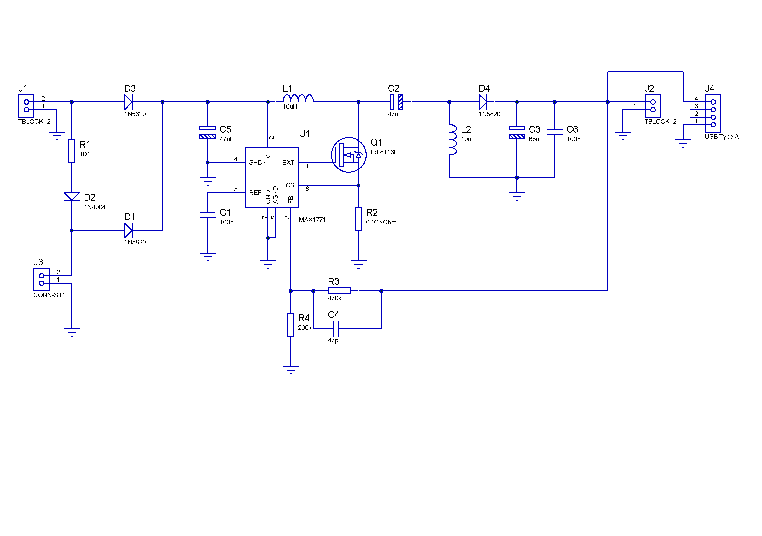
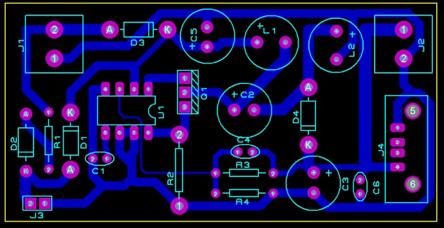
Rev 1 Schematic
It might be very slow , but it is also very safe at a sub C/30 charge rate no special precautions need to be made to NiMh batteries.
The sepic topology allows the raspberry pi be powered from a voltage higher or lower than the output voltage, Ideal for being powered from a 9V wall wart or a 4 Cell Stack and producing a 5V output.
The supplies are diode OR’d together so whichever is the highest supplies the sepic converter, meanwhile the battery is trickle charged by R1 via D2 during normal operation.
During a power failure the battery stack takes over supplying the input to the sepic.
A detailed applications note explains how to design for sepic converters, lets just run through this example for the raspberry pi. In this example we’ll use the MAX1771 as the controller of the converter, it is easily available from the catalogue distributors and available in a DIP for ease of soldering it also has a Max Vin of 16.5V. In the sepic configuration the maximum input is decreased by the output voltage so it should be able to cope with input voltages up to 11.5V.
So let’s look into the design for the raspberry pi power supply we want to achieve the following key specifications.
Vout = 5V
Iout = 0.8A
Vin = 3.2V-11.5V
So following the application note for some of the critical components gives
Step 1 :- Duty Cycle Calculation
Lets assume the diode drop is 0.4V
Dmax= (Vout+ Vd)/(Vin(min)+Vout +Vd)
Dmax= ( 5 + 0.4)/(3.2 + 5 + 0.4)
Dmax = 0.63
Step 2 :- Calculate the inductor currents
Calculate the current in L1
I= Iout * (Vout/Vin(min)) * DC
I= 0.8 *(5 / 3.2) * 0.63
I = 0.78 A
Next lets calculate the inductance for ease of sourcing from the catalogue suppliers in this design we will use separate inductors instead of a coupled inductor.
L1 = L2 = L = (Vin(min) / (I * Fsw )) * Dmax
= (( 3.2 ) / ( 0.78 * 300000))*0.63
= 8.6 uH
Calculating out the peak current in L1
I(L1) = IOUT * ((VOUT + Vd) / Vin(min)) * (1 + Dmax.2)
= 0.8 * ((5 + 0.4) / 3.2) * (1 +0.32)
= 1.78 A
Calculate the peak current in L2
I(L2) = IOUT * (1 + Dmax/2)
= 0.8 * 1.32
= 1.05 A
So now we know the main specs for the inductor, looking farnell murata has a10uH inductor the 13R103C looks like it comfortably meets the requirements with some headroom, and they usually have them in stock (A big deal for inductors if you only want a few...).
Step 3:- Calculate Mosfet parameters
Mosfet Peak Current is the sum of the peak currents in the inductor so 1.05 + 1.78 = 2.83A and the rated drain voltage needs to be greater than Vin+Vout or 11.5V + 5V = 16.5V
For capacitors I selected the Sanyo Oscon family these are becoming harder to find but pay attention to getting the best ESR capacitors for a sepic convertor especially for the transfer capacitor.
The circuit is designed on a single layer PCB shown below :-
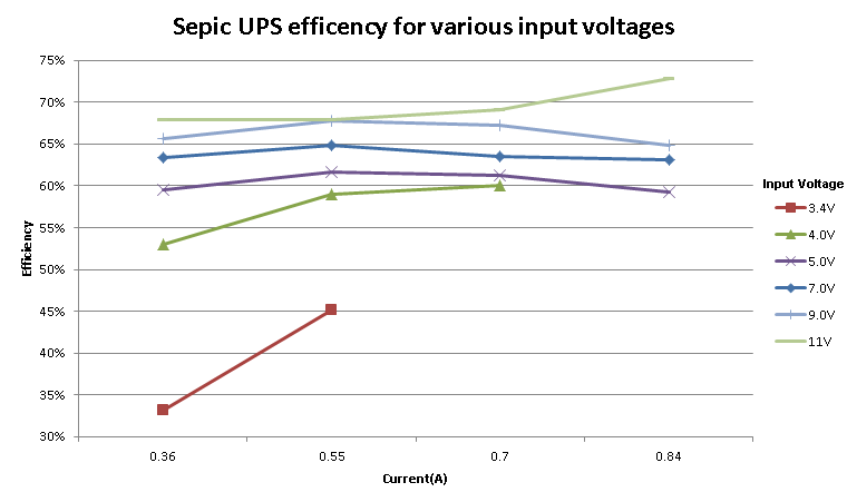
How did it all work out below is an efficiency plot I measured in the lab showing the efficiency at various input voltages and currents
The bill of materials for this project is hyperlinked to Farnell for some of the more unusual components
Note that C2,C3 and C5 need to be low ESR I used the sanyo oscon family, they are expensive but necessary especially for C2.
A note on FET’s originally this design used IRL8813L this worked well with the first few batches of FET’s but I had a batch that wasn’t working to well at low voltages and the big gate capacitance was killing the gate drive, plus they where pricey so instead I’ve changed to the IPP114N03L from infineon which seems to work well, it has a much lower gate capacitance and acceptable Ron.
Bill Of Materials
=================
QTY PART-REFS VALUE
--- --------- -----
Resistors
---------
1 R1 100
1 R2 0.025 Ohm
1 R3 470k
1 R4 200k
Capacitors
----------
1 C1 100nF
2 C2,C5 47uF Needs to be low ESR 68uF works fine as well
1 C3 68uF Needs to be low ESR
1 C4 47pF
Integrated Circuits
-------------------
1 U1 MAX1771
Transistors
-----------
1 Q1 IPP114N03L
Inductors
-----------
2 L1,L2 10uH 13R103C
Diodes
------
3 D1,D3,D4 1N5820
1 D2 1N4004
Miscellaneous
-------------
2 J1,J2 TBLOCK-I2
1 J3 CONN-SIL2
1 J4 USB Type A