![]()
When the P-Type and N-Type materials are joined together a diode is formed. A diode will allow electricity to flow in one direction only, rather like a valve.
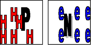
The following will explain briefly how the diode can function. When the different materials, P-type and N-type, are physically joined together a junction is formed. At this junction the electrons from the N-Type material will jump across and fill in the Holes in the P-Type material. In this immeduate area the charge carriers are removed or depleted and a Depletion layer is formed. This is illustrated here.
This Depletion layer forms before any power supply or battery is applied across the diode. To get the diode conducting there will need to be at least 0.6 volts applied to overcome this Depletion Layer as it forms what is referred to as a "Potential Barrier" (This 0.6V is the min. voltage required for a Silicon Diode. The Value is 0.3-0.4V for a Germanium type diode)
There are two methods of connecting a Diode. The first is referred to as "Forward Biased" and the second is "Reversed Biased"modes.