 |
|
|
| |
| EIA RS-449 |
 |
| RS449 redefines RS232 and was intended to replace
it . This recommendation includes several CCITT V.24 circuits which were not
included in RS-232 and they are 140,141,142,126,116 and 117. |
| It also specifies that for data rates higher than
20Kb/s ten V.24 circuits should have balanced circuits and use V.11 / RS422
voltage levels making them compatable with CCITT X.21 . |
| These ten circuits are
103,104,105,106,107,108,109,113,114 and 115 , thus there are ten return
circuits defined for these . |
| The remaining V.24 circuits are unbalanced
(V.10/RS-423a) with a single common return.The recommended connector for RS-449
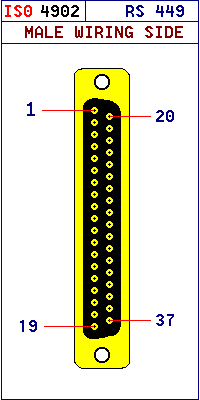
is a 37 pin D-Type complying to ISO 4902. |
|
| RS 449 Pin Designations |
|
| PIN |
CIRCUIT |
DESCRIPTION |
| 1 |
SHIELD |
Ground |
| 2 |
SI |
Signalling Rate Indicator |
| 3 |
|
|
| 4 |
SD(A) |
Send data |
| 5 |
ST(A) |
Send timing |
| 6 |
RD(A) |
Receive data |
| 7 |
RS(A) |
Request to send |
| 8 |
RT(A) |
Receive Timing |
| 9 |
CS(A) |
Clear to send |
| 10 |
LL |
Local loopback |
| 11 |
DM(A) |
Data mode |
| 12 |
TR(A) |
Terminal Ready |
| 13 |
RR(A) |
Receiver ready |
| 14 |
RL |
Remote Loopback |
| 15 |
IC |
Incoming call |
| 16 |
SF/SR |
Select Frequency / Sig Rate Selecter |
| 17 |
TT(A) |
Terminal timing |
| 18 |
TM |
Test mode |
| 19 |
SG |
Signal ground
common |
| 20 |
RC |
Receive common |
| 21 |
|
|
| 22 |
SD(B) |
Send data |
| 23 |
ST(B) |
Send timing |
| 24 |
RD(B) |
Receive data |
| 25 |
RS(B) |
Request to send |
| 26 |
RT(B) |
Receive timing |
| 27 |
CS(B) |
Clear to send |
| 28 |
IS |
Terminal in service |
| 29 |
DM(B) |
Data mode |
| 30 |
TR(B) |
Terminal ready |
| 31 |
RR(B) |
Receiver ready |
| 32 |
SS |
Select Standby |
| 33 |
SQ |
Signal Quality |
| 34 |
NS |
New Signal |
| 35 |
|
|
| 36 |
|
|
| 37 |
|
|
|
|
| |
|
| |
| |
|
| |
|
